Chip assembly and packaging increasingly complex
Semiconductor packaging is making a difference in 5G and 6G communications, optical networks, health sensors, automotive engineering, you name it! The assembly and packaging of chips is becoming increasingly difficult. That's why HAN offers the Semiconductor Packaging course as a full-time program for undergraduates, but also as a part-time course for professionals. Semiconductor packaging is a subject that’s drawing ever more attention. Why?

Even students from Panama
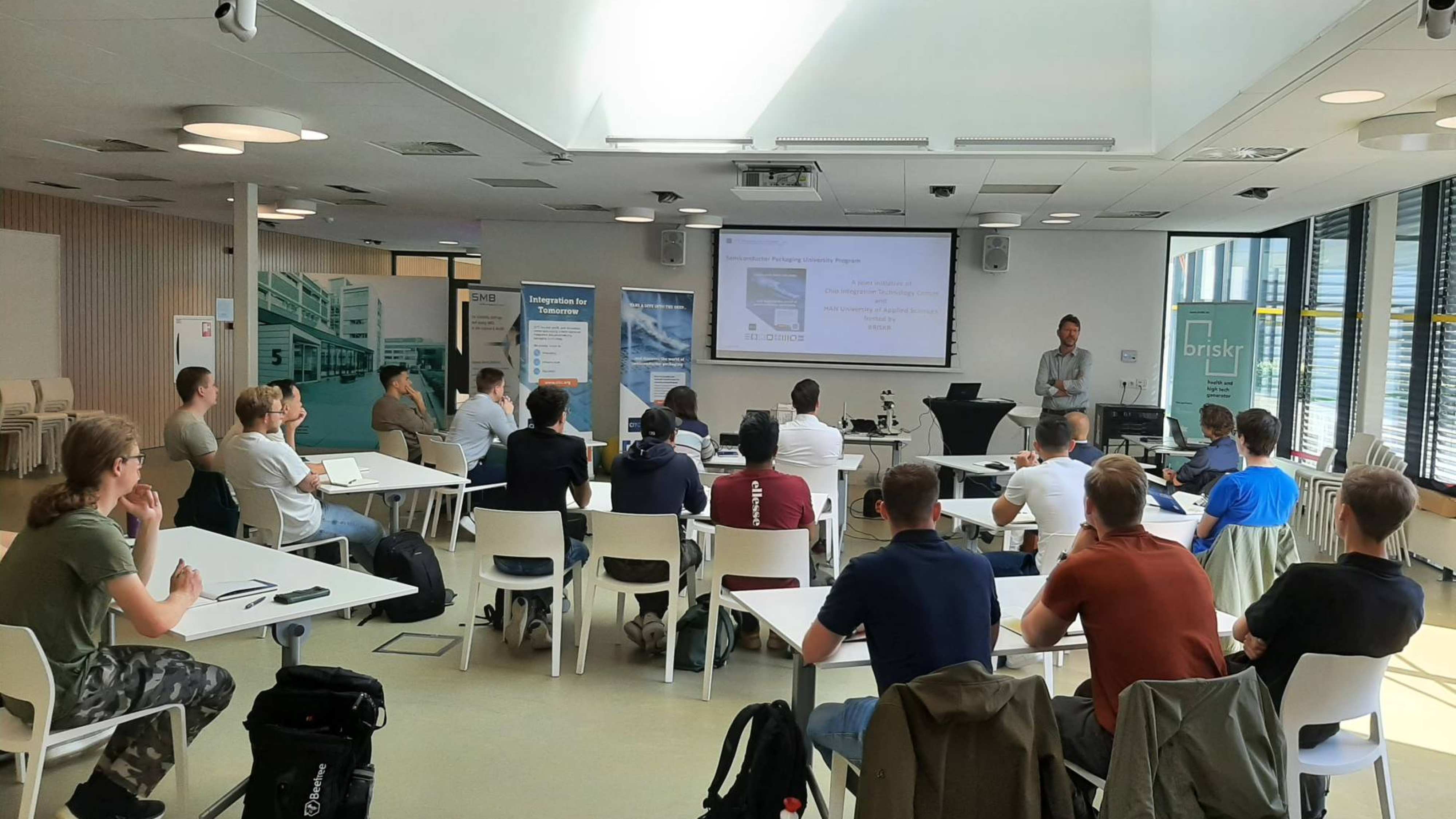
On behalf of both HAN Engineering and Automotive and CITC (Chip Integration Technology Center), Joop Bruines is responsible for the content and implementation of the Semiconductor Packaging University Program.
In addition to HAN and CITC, various other organizations are involved behind the scenes: NXP, Nexperia, Ampleon, TNO and the TU Delft.
Bruines: "This program, which will start for the 4th time, has 15 participants. I think that's a nice number. They come from all kinds of disciplines, such as automotive, electrical and mechanical engineering, chemistry, and mechatronics. If you include the part-time course for professionals, the total number of participants is 49." About half of them are physically present at the Noviotech Campus in Nijmegen. The other half participate online.
"Participants come from various countries, including Sweden, Italy, France, Germany, India and even Panama," Bruines says. "I’ve had several interesting calls with the technical university in Panama. The country wants to be prepared for the eventuality that the U.S. wants to bring the chip industry closer to home. Training will be important then, which is why we have participants from Panama."

Exchange program
The undergraduate exchange is full-time. Students attend the on Monday sessions and they also take a practical component, provided by CITC and NXP.
Integrated optics and antennas
The lecturers are industry experts, a deliberate choice carried on from when the course started in 2020. "Some topics are still the same as they were then; in other areas the course has developed. Compared to the 1st year, there is now more focus on current topics such as integrated optics and antennas."
Importance of this unique course
More and more companies are recognizing the importance of this unique course. "Chip manufacturing has undergone all kinds of developments. Frequencies are getting higher with 5G and 6G. Cars also increasingly use radars and are mostly electrically powered. This has numerous implications for the assembly and packaging of chips. That's getting harder and harder."
"It used to be, simply put, a matter of attaching wires and putting plastic over it. Now, more and more consideration is being given to packaging right from the initial design of a chip so that it does not interfere with the chip's performance. With optical chips, this is even more true," Bruines explains.
Very multidisciplinary
According to Bruines, Semiconductor Packaging is very multidisciplinary. "It overlaps with electronics, chemistry, mechanical engineering and materials science. You can only get it right if different parties work together. In this case, the initiative came from industry. In other cases, where that cooperation is lacking, you can’t get something like this off the ground. The Netherlands is also very strong in the area of packaging. We have many great companies, which we also visit during the course."
Source: Lifeport.nl
Photography: Christian Ketelaars (CITC)
Contact us
Want to know more about the Semiconductor Packaging program?
- Please contact Joop Bruines at Joop.Bruines@han.nl
